High-Density Interconnect (HDI) PCBs represent a significant leap in electronic miniaturization and performance, enabling the creation of increasingly complex and compact devices. Among their myriad applications, one stands out as particularly transformative: their pivotal role in the evolution of modern mobile devices, especially smartphones. The relentless demand for thinner, lighter, and more powerful smartphones has driven manufacturers to push the boundaries of PCB technology, and HDI PCBs have emerged as the cornerstone of this innovation.
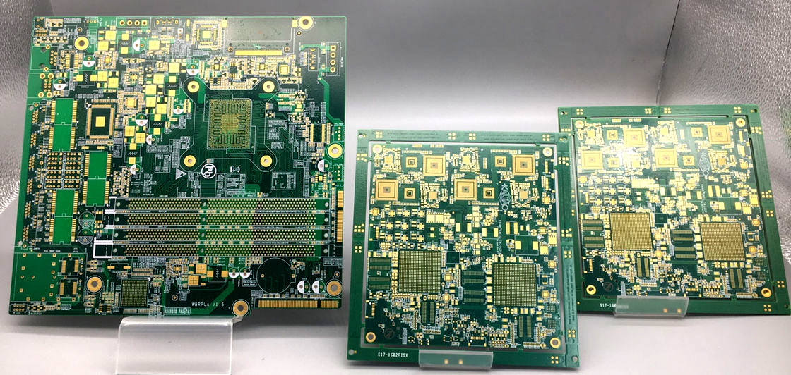
The core advantage of HDI PCBs lies in their ability to pack more circuitry into a smaller space. This is achieved through the use of microvias, blind and buried vias, and finer lines and spaces, allowing for denser component placement and improved signal integrity. In smartphones, this translates to a smaller motherboard, freeing up valuable internal space for larger batteries, improved cameras, and other advanced components. Without HDI technology, the slim and feature-rich smartphones we rely on today would be simply impossible.
The complexity of modern smartphone processors, memory chips, and communication modules necessitates intricate interconnections. HDI printed circuit boards provide the necessary density to route these signals efficiently, minimizing signal loss and crosstalk, which are critical for high-speed data transfer and reliable performance. The ability to integrate multiple layers and components within a compact footprint enables the creation of highly integrated system-on-chips (SoCs), which are the brains of modern smartphones. These SoCs handle everything from processing power and graphics to connectivity and AI functions, all within a tiny package made possible by advanced HDI design.
Furthermore, HDI PCBs play a crucial role in the miniaturization of camera modules, which are becoming increasingly sophisticated in smartphones. High-resolution sensors, multiple lenses, and advanced image processing capabilities require complex interconnections and high-density packaging. HDI technology allows for the precise placement and routing of these components, ensuring optimal image quality and performance. The ability to integrate multiple camera modules into a single device, enabling features like optical zoom and depth sensing, is a testament to the capabilities of HDI PCBs.
Beyond processing and imaging, HDI PCBs are essential for the integration of advanced connectivity features in smartphones. 5G connectivity, Wi-Fi 6, and Bluetooth 5.0 require high-frequency signals and complex antenna designs. HDI technology enables the creation of compact and efficient antenna systems, as well as the routing of high-speed signals with minimal loss. This ensures that smartphones can deliver seamless connectivity and fast data transfer speeds, even in crowded environments.
The impact of HDI PCBs extends beyond smartphones to other mobile devices, such as tablets, smartwatches, and laptops. These devices also benefit from the miniaturization and performance advantages offered by HDI technology, enabling the creation of thinner, lighter, and more powerful products. In the wearable technology sector, where size and weight are critical factors, HDI PCBs are indispensable for creating compact and functional devices.
In conclusion, the most significant application of HDI PCBs is undoubtedly in the evolution of modern mobile devices, particularly smartphones. Their ability to enable miniaturization, enhance performance, and facilitate the integration of advanced features has revolutionized the way we communicate, access information, and interact with the world. As mobile technology continues to advance, HDI PCBs will remain a critical enabler, driving innovation and shaping the future of electronic devices. The continued refinement and development of HDI technology will be essential to meet the ever-increasing demands of the consumer electronics market.